Papers
A high-swing, high-impedance MOS cascode circuit
- regulated cascode (or RGC) achieves higher output impedance than simple cascode.
- RGC has larger output voltage range than optimally biased simple cascode.
The active-input regulated-cascode current mirror
Ultra high-compliance CMOS current mirrors for low voltage charge pumps and references
Relationship between frequency response and settling time of operational amplifiers
Amplifiers, source followers and cascodes
024: Single-transistor amplifier
\[A_v = g_m r_{DS} = \dfrac{2 I_{DS}}{V_{ov}} \cdot \dfrac{V_E L}{I_{DS}} = \dfrac{2 V_E L}{V_{ov}}\]- high gain needs large \(L\) and high \(g_m/i_d\)
0213: Miller capacitance feedback effects
- the \(C_{gd}\) miller capacitor gives a positive zero:
- the gain magnitude becomes constant at high frequency, since the transistor is diode connected with impedance \(1/g_m\)
- the phase becomes in-phase at high frequency instead of completely-out-of-phase at low frequency
- such a phenomenon can only be explained by a positve zero after the negative pole
- full small-signal analysis reveals that \(f_z = \dfrac{g_m}{2\pi C_F}\)
0250: Cascode with resistive load
- cascode convert current to voltage, the gain will be larger if the load resistance is larger.
- however, in reality the gain cannot increase to infinity, to see the limit we have to include the \(R_B\) and \(r_{DS}\).
Stability of Operational amplifiers
0515: What makes an opamp an opamp?
An opamp is really a single-pole system. As a result, it allows exchange of gain with bandwidth, within a specific GBW.
Usually the number number of high impedance nodes indicates the number of poles, there can be only one internal node at high impedance for opamp.
All two-stage amplifiers have two high-impedance nodes and hence two poles. Therefore, all amplifiers with two high-impedance nodes are called two-stage amplifiers, irrespective of the number of transistors.
Wideband amplifiers are very different. They consist of more stages, each of them having a pole. They are normally compensated at one particular setting of the gain. They are not meant to exchange gain for bandwidth.
0526: Relation PM, damping and \(f_2/\text{GBW}\)
| \(\dfrac{f_2}{\text{GBW}}\) | PM (\(^\circ\)) | \(\zeta = \dfrac{1}{2}\sqrt{\dfrac{f_2}{GBW}}\) | \(P_f\) (dB) | \(P_t\) (dB) |
|---|---|---|---|---|
| 0.5 | 27 | 0.35 | 3.6 | 2.3 |
| 1 | 45 | 0.5 | 1.25 | 1.3 |
| 1.5 | 56 | 0.61 | 0.28 | 0.73 |
| 2 | 63 | 0.71 | 0 | 0.37 |
| 3 | 72 | 0.87 | 0 | 0.04 |
When designing opamp we will try to avoid peaking. Thus \(72^\circ\) PM is a good safety position to start with, as all parasitic capacitances come in after layout, pushing the non-domiant pole to lower values and decreasing the phase margin. Eventually \(63^\circ\) PM is good enough to not have peaking in the frequency domain.
Another reason for \(63^\circ \sim 72^\circ\) PM is that it is a good compromise between peaking and bandwidth; Larger PM reduces the bandwidth too much.
0530: Generic 2-stage opamp
\(GBW = \dfrac{g_{m1}}{2\pi C_c}\), since node 1 is virtual ground, and the output voltage is generated by the current flow through \(C_c\).
\(f_{nd} = \dfrac{g_{m2}}{2\pi C_L}\), since at high frequency \(C_c\) is shorted, the non-domiant pole is calculated by the impedance at node 1.
\(f_z = \dfrac{g_{m2}}{2\pi C_c}\), this is a positive zero.
Systematic Design of Operational Amplifiers
Basics
Differential Pair
\[A_v = - g_m R_D\]CMRR
\[CMRR = \dfrac{\vert A_{DM} \vert}{\vert A_{CM-DM} \vert}\] \[\vert A_{CM-DM}\vert_1 = \left\vert \dfrac{\Delta R_c}{1/g_m + 2 R_{EE}} \right\vert\] \[\vert A_{CM-DM}\vert_1 = \left\vert \dfrac{\Delta g_m R_c}{1+2g_mR_{EE}} \right\vert\] \[\vert A_{CM-DM} \vert = \sqrt{\vert A_{CM-DM} \vert_1^2 + \vert A_{CM-DM}\vert_2^2}\]Offset
\[V_{os,1} = \dfrac{(V_{GS}-V_{TH})\Delta R_D}{2 R_D}\] \[V_{os,2} = \dfrac{(V_{GS}-V_{TH})\Delta\left(\dfrac{W}{L}\right)}{2\left(\dfrac{W}{L}\right)}\] \[V_{os,3} = \Delta V_{TH}\] \[V_{os} = \sqrt{V_{os,1}^2+V_{os,2}^2+V_{os,3}^2}\]Current Mirror Load
\[A_v = g_m (r_{on}\Vert r_{op})\]Frequency Response (Lecture 6)
\[H(s) = A_v \cdot \dfrac{(1+s/\omega_{z,1})\dots (1_s/\omega_{z,n})}{(1+s/\omega_{p,1}) \dots (1+s/\omega_{p,n})}\]Coupling Capacitor and Bypass Capacitor
The approximated method:
- Each capacitor generates (exactly) one pole and one zero.
- The zero may degenerate to zero or infinite frequency.
- The pole frequency is found by RC time constant.
- The zero frequency is found by finding the frequency when the output is zero (when all the other capacitors are working ideally small or large).
Miller Effect
LHP zero is okay. RHP zero is dangerous.
Open Circuit Time Constant (Lecture 8)
Common Source
Common Gate (Lecture 9)
Common Drain (Lecture 10)
Differential Pair
Feedback (Lecture 13)
Operational Amplifier
Two Stage Amplifier
Slew Rate
PSRR
Folded Opamp
Limiter
CMFB
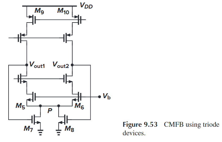
One of the CMFB is using triode devices. The M7 and M8 will be in deep triode region, such that the current sources M5 and M6 are degenarated. Assume the current sources M5 and M6 are bigger than M9 and M10, then the output common mode will be lower than nomimal output CM level. The gate voltage of M7 and M8 will decrease, and their resistance will increase, the current of M5 and M6 will decrease.
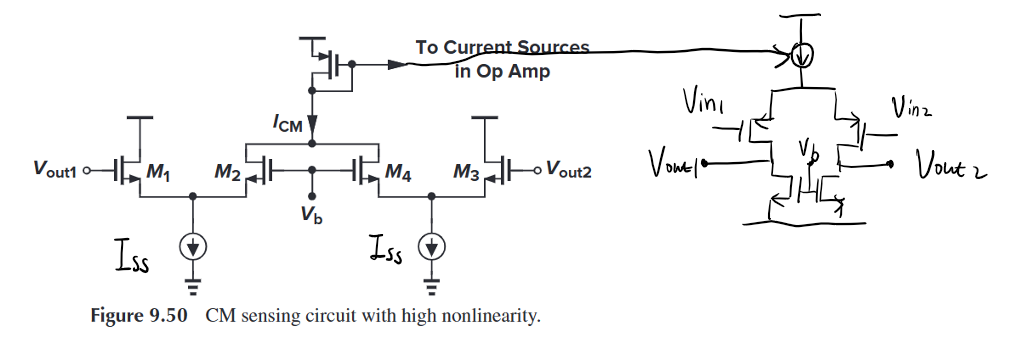
Another way of CMFB is using a differential pair to generate a current.
Digital Circuits
SR Latch
D-Flip Flop
C2MOS Latch
CML Latch
Impedance Formula
\[R \Vert \dfrac{1}{sC} = \dfrac{R}{1+sRC}\]Impedance Transformation
Series-to-Parallel
Inductor
\[Q = \dfrac{\omega L_s}{R_s}\] \[R_p = R_s(1+Q^2)\] \[L_p = L_s (1+\dfrac{1}{Q^2})\]Capacitor
\[Q = \dfrac{1}{\omega R_s C_s}\] \[R_p = R_s(1+Q^2)\] \[C_p = \dfrac{C_s}{1+\dfrac{1}{Q^2}}\]Parallel-to-Series
Inductor
\[Q = \dfrac{R_p}{\omega L_p}\] \[R_s = \dfrac{R_p}{1+Q^2}\] \[L_s = \dfrac{L_p}{1+\dfrac{1}{Q^2}}\]Capacitor
\[Q = \omega R_p C_p\] \[R_s = \dfrac{R_p}{1+Q^2}\] \[C_s = C_p (1+\dfrac{1}{Q^2})\]High-Q System
For inductor
\[Q = \dfrac{\omega L_s}{R_s} = \dfrac{R_p}{\omega L_p}\]if \(Q\) is large, \(L_s \approx L_p\) (with error \(1 + \dfrac{1}{Q^2}\))
\[R_s R_p = (\omega L)^2\]For capacitor
\[Q = \dfrac{1}{\omega R_s C_s} = \omega R_p C_p\]if \(Q\) is large, \(C_s \approx C_p\) (with error \(1 + \dfrac{1}{Q^2}\))
\[R_s R_p = \dfrac{1}{(\omega C)^2}\]Oscillator
Barkhausen Criteria
When the oscillator just starts to oscillate, we can use small signal model. If the closed-loop transfer function is
\[H(s) = \dfrac{A(s)}{1+A(s)\beta(s)}\]It must be unstable at the equilibrium point, thus from the concept of gain margin
\[\begin{align} \angle A(j\omega_{\text{x}})\beta(j\omega_{\text{x}}) &= -180^\circ\\ \vert A(j\omega_{\text{x}})\beta(j\omega_{\text{x}}))\vert &> 1 \end{align}\]Wien-Bridge Oscillator
we assume the input is at
let
\[\begin{align} Z_p &= \dfrac{R}{1+sRC}\\ Z_s &= R + \dfrac{1}{sC} \end{align}\]the closed-loop transfer function can be calculated as
\[H(s) = \dfrac{V_{out}(s)}{V_{in}(s)} = \dfrac{(R_1 + R_2)/R_1}{1 - \dfrac{R_2}{R_1} \dfrac{Z_p}{Z_s}}\] \[\dfrac{R_2}{R_1} \dfrac{Z_p}{Z_s} = \dfrac{R_2}{R_1} \dfrac{j\omega RC}{1-\omega^2 R^2C^2 + 2j\omega RC}\] \[\omega_x = \dfrac{1}{RC}\] \[\dfrac{R_2}{2R_1} > 1\]Colpitts Oscillator

Self-Charged XO
- The sine wave will first be converted to square wave, with the requirement that the output will trip exactly in the middle of the input voltage swing. A self-adaptive boby-biasing technique is used.
Flicker Noise
\[A \cdot \dfrac{f_c}{f}\] \[1.38 A \cdot \dfrac{f_c}{f_{min}} \sum_{n=0}^{N_{max}} \dfrac{10^{-n}}{1+(\dfrac{f}{10^n f_{min}})^2}\]Phase Detector
Harmonic-Rejection Mixer
A mixer can be used as a phase detector.
\[\cos(\omega t) \cdot \cos(\omega t + \phi) = \dfrac{1}{2} \cdot \cos\left( 2\omega t + \phi\right) + \dfrac{1}{2} \cdot \cos\phi\]When mixing two sinosoidal signal, there is no higher harmonics.
\[\cos(\omega_1 t) \cdot \cos(\omega_2 t) = \dfrac{1}{2} \cdot \cos\left( (\omega_1 + \omega_2) t\right) + \dfrac{1}{2} \cdot \cos\left( (\omega_1 - \omega_2) t\right)\]When mixing sinosoidal with square wave, there is higher harmonics.
\[f_1(t) = \cos(\omega t) - \dfrac{1}{3} \cos(3\omega t) + \dfrac{1}{5} \cos(5\omega t) - \dfrac{1}{7} \cos(7\omega t) + \dots\]If we have available different phase (\(\pm 45^\circ\)) of \(f_1(t)\)
\[\begin{align} f_2(t) &= f_1\left(t+\dfrac{T}{8}\right)\\ &= \cos(\omega t + \pi/4) - \dfrac{1}{3}\cos(3\omega t + 3 \pi /4) + \dfrac{1}{5}\cos(5\omega t + 5\pi/4) + \dots\\ &= \dfrac{1}{\sqrt{2}} \left( \left(\cos(\omega t)-\sin(\omega t)\right) +\dfrac{1}{3}\left(\cos(3\omega t) + \sin(3\omega t)\right) - \dfrac{1}{5}\left( \cos(5\omega t) - \sin(3\omega t) \right) \right) \end{align}\] \[\begin{align} f_3(t) &= f_1\left(t-\dfrac{T}{8}\right)\\ &= \cos(\omega t - \pi/4) - \dfrac{1}{3}\cos(3\omega t - 3 \pi /4) + \dfrac{1}{5}\cos(5\omega t - 5\pi/4) + \dots\\ &= \dfrac{1}{\sqrt{2}} \left( \left(\cos(\omega t)+\sin(\omega t)\right) +\dfrac{1}{3}\left(\cos(3\omega t) - \sin(3\omega t)\right) - \dfrac{1}{5}\left( \cos(5\omega t) + \sin(3\omega t) \right) \right) \end{align}\]thus using \(\sqrt{2}f_1(t) + f_2(t) + f_3(t)\) can cancel third and fifth harmonics.
Crystal Oscillator
Resonant Frequency
We want to calculate the resonant frequency of a crystal, including \(C_0, R_m, L_m, C_m\). By definition, resonat frequency is the frequency such that the total impedance is purely real.
\[Z_0 = -\dfrac{j}{\omega C_0}\] \[Z_m = R_m + j\omega L_m - \dfrac{j}{\omega C_m}\] \[Z_p = \dfrac{Z_0 Z_m}{Z_0 + Z_m} = \dfrac{\dfrac{L_m}{C_0} - \dfrac{1}{\omega^2 C_0 C_m} - \dfrac{j R_m}{\omega C_0}}{R_m + j\left(\omega L_m - \dfrac{1}{\omega C_m} - \dfrac{1}{\omega C_0}\right)}\]The condition for \(Z_p\) to be purely real
\[\dfrac{-\dfrac{R_m}{\omega C_0}}{\dfrac{L_m}{C_0}-\dfrac{1}{\omega^2 C_0 C_m}} = \dfrac{\omega L_m - \dfrac{1}{\omega C_m} - \dfrac{1}{\omega C_0}}{R_m}\]Solving the equatoin, we can find two resonant frequency
\[\omega_s \approx \dfrac{1}{\sqrt{L_m C_m}}\] \[\begin{align} \omega_a \approx \dfrac{1}{\sqrt{L_m \left(C_m \Vert C_0\right)}} \approx \dfrac{1}{\sqrt{L_m C_m}} \left(1+\dfrac{C_m}{2C_0}\right) \end{align}\]If there are load capacitance, the load capacitance \(C_L\) will be parallel with \(C_0\), thus
\[\omega_s \approx \dfrac{1}{\sqrt{L_m C_m}}\] \[\omega_a \approx \dfrac{1}{\sqrt{L_m \left(C_m \Vert \left(C_0+C_L\right)\right)}} \approx \dfrac{1}{\sqrt{L_m C_m}} \left(1+\dfrac{C_m}{2(C_0+C_L)}\right)\]Depending on how the oscillator is designed, the oscillation frequency will be betwenn the two value (this is stated by many books, I didn’t know the real reason for this statement though).
\[\omega_s \le \omega_{osc} \le \omega_a\]Equivalent Resistance
Let’s denote \(jX = j\omega L_m - \dfrac{j}{\omega C_m}\), and \(j X_{C0} = -\dfrac{j}{\omega C_0}\). The total impedence of the crystal (note that the load \(C_L\) is not included)
\[\begin{align} Z &= \dfrac{\left(R_m + jX\right)\left(j X_{C0}\right)}{R_m + j(X+X_{C0})}\\ &= \dfrac{R_m X_{C0}^2}{R_m^2 + \left(X+X_{C0}\right)^2} + \dfrac{jX_{C0}\left[R_m^2 + X\left(X+X_{C0}\right)\right]}{R_m^2 + \left(X+X_{C0}\right)^2} \end{align}\]The effective resistance is given by
\[R_e = \dfrac{R_m X_{C0}^2}{R_m^2 + \left(X+X_{C0}\right)^2}\]consider when we sweep the frequency from \(\omega_s\) to \(\omega_a\), formally \(\dfrac{1}{\sqrt{L_m C_m}} \le \omega \le \dfrac{1}{\sqrt{L_m C_m}} \left(\dfrac{C_m}{2(C_0+C_L)}\right)\). The effective resistance will increase from
\[R_e\vert_{\omega=\omega_s} \approx R_m\]to
\[\begin{align} R_e\vert_{\omega=\omega_a} &\approx R_m \left(\dfrac{C_L+C_0}{C_L}\right)^2 \end{align}\]