Inductor Simulation
using sp or psp simulation to simulate inductor, we calculate the Z parameter
In virtuoso
1
2
3
4
5
Imagz = imag(zpm('psp 1 1)) + imag(zpm('psp 2 2)) - imag(zpm('psp 1 2)) - imag(zpm('psp 2 1))
Ls = Imagz / 2 / 3.14 / xval(Imagz)
Rs = real(zpm('psp 1 1)) + real(zpm('psp 2 2)) - real(zpm('psp 1 2)) - real(zpm('psp 2 1))
Q = Imagz / Rs
Rp = (1+Q*Q)*Rs
Capacitor Simulation
\[C_s = -\dfrac{1}{2\pi f} \cdot \dfrac{1}{Im(Z_{diff})}\] \[R_s = Re(Z_{diff})\]Phase Noise
References:
A Charge-Sharing Locking Technique With a General Phase Noise Theory of Injection Locking
Reference phase noise
\[\begin{align} \mathcal{L}_{ref}(f) &= \dfrac{1}{2} S_{\phi} = \dfrac{1}{2} S_{t} (2\pi F_{ref})^2\\ &= \dfrac{1}{2} \cdot \dfrac{\sigma_{t}^2}{F_{ref}/2} \cdot (2\pi F_{ref})^2\\ &= 4\pi^2 F_{ref} \cdot \sigma_{t}^2 \end{align}\]For example, \(\sigma_t = 112.5 \,\mathrm{ fs}\) with \(F_{ref} = 200\,\mathrm{ MHz}\), \(\mathcal{L}_{ref} = -160 \,\mathrm{ dBc/Hz}\).
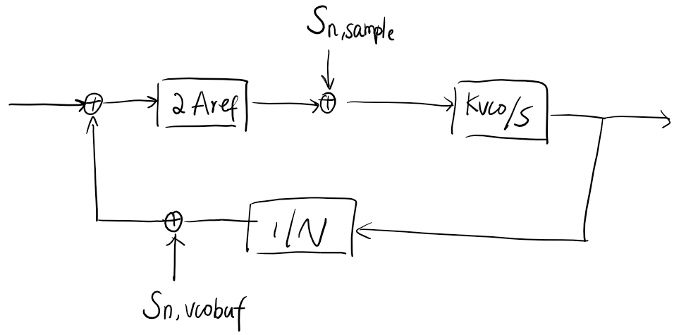
However, this is the reference phase noise in the reference frequency domain. To the output it will be multiplied by \(N^2\) and low-passed by the loop filter.
VCO phase noise
\[\begin{align} \mathcal{L}_{osc}(f) &= \dfrac{1}{2} S_{\phi} = \dfrac{1}{2}S_t (2\pi F_{osc})^2\\ &= \dfrac{1}{2} \cdot \dfrac{\sigma_t^2}{F_{osc}/2} \cdot \left(\dfrac{F_{osc}}{2\pi f}\right)^2 \cdot (2\pi F_{osc})^2\\ &= \sigma_t^2 \cdot \dfrac{F_{osc}^3}{f^2} \end{align}\]For example, \(\sigma_t = 1 \,\mathrm{fs}, F_{osc} = 10\,\mathrm{GHz}, f = 10\,\mathrm{MHz}\), \(\mathcal{L}_{osc}(f) = -140\,\mathrm{dBc/Hz}\).
Fractional-N PLL quantization noise:
BBPLL Theory
Multirate time-domain model
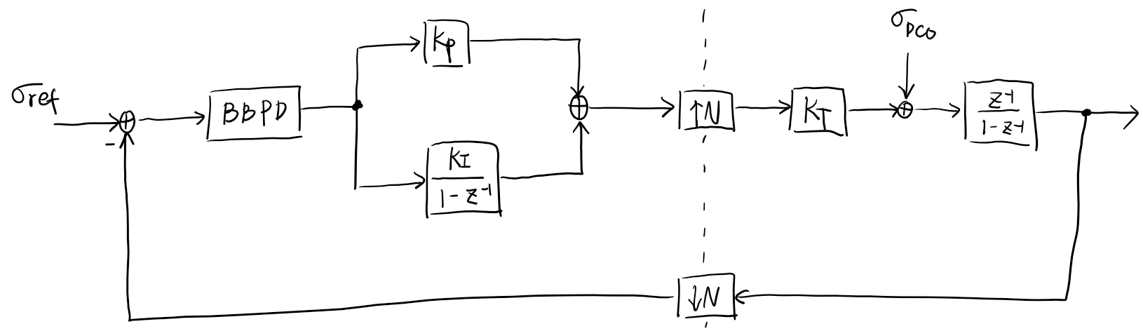
Convert to single-rate model
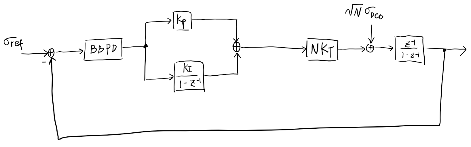
Equivalent linear model
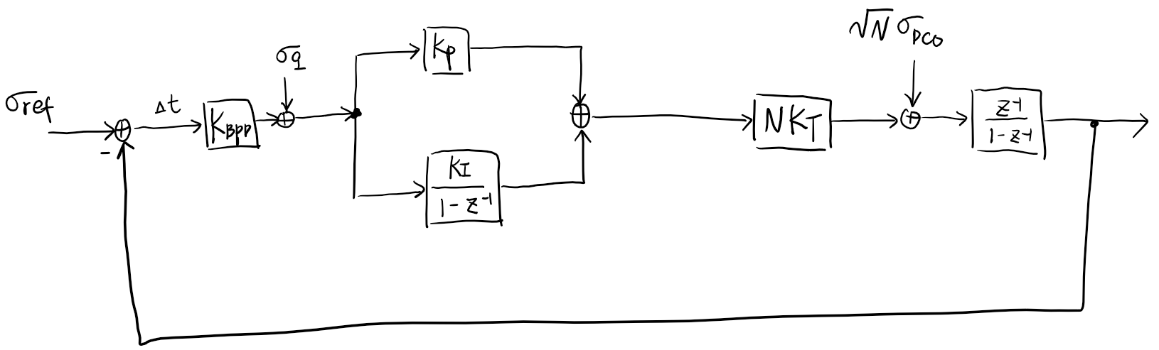
Under some assumption, approximately
\[K_{BPD} = \sqrt{\dfrac{2}{\pi}} \cdot \dfrac{1}{\sigma_{\Delta t}}\] \[\sigma_q^2 = 1 - K_{BPD}^2 \cdot \sigma_{\Delta t}^2 = 1 - \dfrac{2}{\pi}\]Given \(\sigma_{ref}, \sigma_{DCO}, K_P, K_I, N, K_T\), we want to find the value of \(K_{BPD}\). For simplicity, we assume \(K_I\) is very small (\(K_I \ll K_P\)) such that we can ignore it. And we denote \(\chi = N K_{BPD} K_P K_T\).
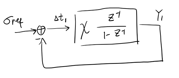
since \(Y_1[k]\) and \(\sigma_{ref}[k]\) are independent
\[\sigma_{Y_1}^2 = (1-\chi)^2 \sigma_{Y_1}^2 + \chi^2 \sigma_{ref}^2\] \[\sigma_{Y_1}^2 = \dfrac{\chi}{2-\chi} \sigma_{ref}^2\] \[\sigma_{\Delta t_1}^2 = \sigma_{ref}^2 + \sigma_{Y_1}^2 = \dfrac{2}{2-\chi} \sigma_{ref}^2\]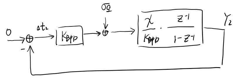
combine with
\[K_{BPD} = \sqrt{\dfrac{2}{\pi}} \cdot \dfrac{1}{\sigma_{\Delta t}}\] \[\sigma_q^2 = 1 - \dfrac{2}{\pi}\]After some algebra (please provide)
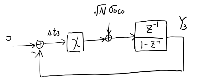
\[\sigma_{\Delta t} = \dfrac{\eta}{2} + \sqrt{\left(\dfrac{\eta}{2}\right)^2 + \sigma_{ref}^2}\] \[\eta = \sqrt{\dfrac{\pi}{2}} \cdot \left(\dfrac{\sigma_{DCO}^2}{2 K_P K_T} + \dfrac{N K_P K_T}{2}\right)\] \[K_{P,opt} = \dfrac{\sigma_{DCO}}{K_T \sqrt{N}}\] \[\eta_{opt} = \sqrt{\dfrac{N \pi}{2}} \sigma_{DCO}\] \[\Delta t[k] = \sigma_{ref}[k] - \sigma_{out}[k]\] \[\sigma_{\Delta t}^2 = \sigma_{ref}^2 + \sigma_{out}^2\] \[\sigma_{out}^2 = \sigma_{\Delta t}^2 - \sigma_{ref}^2\]1
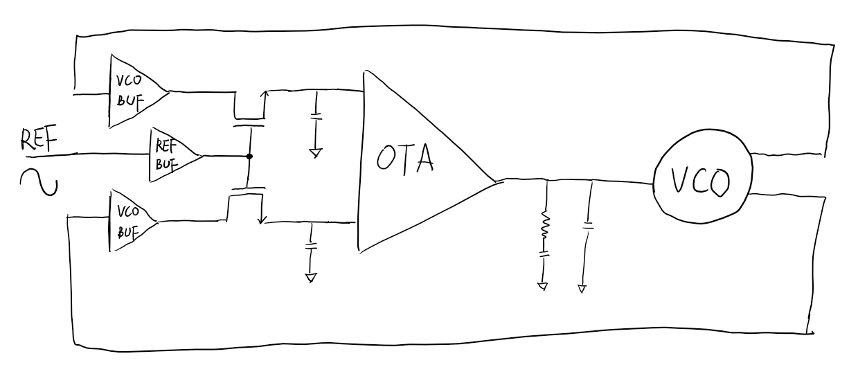
Circuit Design
2
Circuit Design
The circuits is composed of a VCO, a sampler, one reference buffer and two VCO buffer.
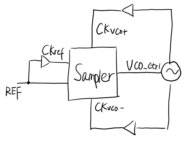
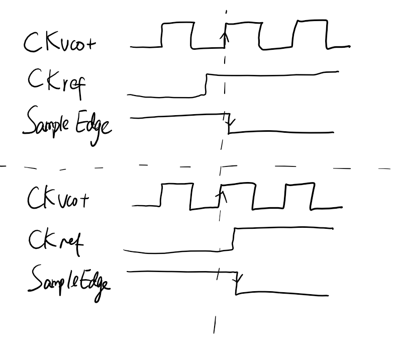
Sampler
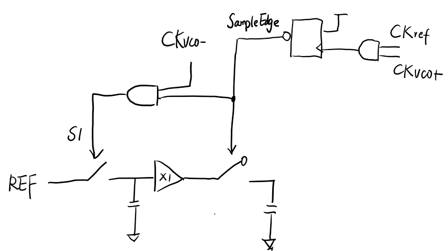
We have to make sure the SampleEdge’s falling edge comes when CKvco- is 0. There are two possibilities, one is CKref asserts when CKvco+ is 0; another one is CKref asserts when CKvco+ is 1. In either case, SampleEdge’s falling edge happens when CKvco+ is 1, then CKvco- is 0.
The diagram shows single-ended sampling, but the real circuits adopts differential sampling.
Reference buffer
The reference buffer is calibrated per die such that CKref transit at the crossover of the reference signal.
Inband Phase Noise Analysis