MOSFET
\[\begin{align} C_{ox} &= \frac{3.9 \epsilon_0}{t_{ox}} = \frac{3.9 \times 8.85e-12}{t_{ox}}\\ I_D &= \frac{1}{2}\mu_n C_{ox} \frac{W}{L}(V_{GS}-V_{TH})^2(1+\lambda V_{DS}) \quad \quad \text{pinch-off region}\\ I_D &= \mu_n C_{ox} \frac{W}{L}\big( (V_{GS} - V_{TH})V_{DS} - \frac{1}{2}V_{DS}^2 \big) \quad \quad \text{triode region} \end{align}\]bode effect (simply remember as source degeneration will have higher threshold voltage).
\[\begin{align} V_{th} = V_{th0} + \gamma (\sqrt{|V_{SB}+2\Phi_F|} - \sqrt{|2\Phi_F|}) \end{align}\] \[\begin{align*} g_m &= \frac{d I_{DS}}{d V_{GS}} = \mu_n C_{ox}\frac{W}{L}(V_{GS} - V_{TH}) = \frac{2 I_{DS}}{V_{GS} - V_{TH}} = \sqrt{2\mu_n C_{ox}\frac{W}{L}I_{DS}}\\ g_{ds} &= \lambda I_{DS} \quad \quad r_o = \frac{1}{\lambda I_{DS}} = \dfrac{L}{L_{typ}} \cdot \dfrac{1}{\lambda_{typ} I_{DS}}\\ g_{mb} &= g_m \dfrac{\gamma}{2\sqrt{2\phi_F + V_{SB}}} \end{align*}\]\(\pi\) Model
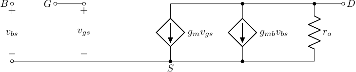 MOSFET \(\pi\) model
- The arrow indicates source of nmos or pmos.
- pmos has the same small signal model as nmos.
- However pmos has source at the top.
- The small signal model is flipped.
\(T\) Model
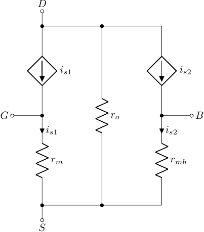 MOSFET \(T\) model
BJT
\[\begin{align} r_{\pi} &= \beta r_m\\ \alpha &= \frac{\beta}{\beta+1}\\ \beta &= \frac{\alpha}{1-\alpha} \end{align}\]Transfer Function
- For a pole at frequency \(\omega_0\), at \(\omega_0 / \sqrt{3}\), the phase drops \(30^\circ\). At \(\omega_0\), the phase drops \(45^\circ\).
- For a first-order transfer function \(H(s) = \dfrac{a + b s}{1 + s \tau}\), the DC gain is \(a\), the prop path is \(\dfrac{b}{\tau}\), with time constant \(\tau\).